Understanding NFC part 1: How It Works and Designing Your Own Reader and Tags
4/30/20257 min read


Yet another NFC tutorial?
If you've ever tried to build an NFC-based project—say, a contactless badge reader, smart lock, or even a simple Arduino-powered tag detector—you’ve probably hit the same wall that many hobbyist electronics designers do: the information is all over the place. One tutorial glosses over the key components, another assumes you already know RF principles, and a dozen more contradict each other on antenna matching and IC selection. And the next 20 tutorials are just copy-paste of each other with the exact same holes in them.
It’s frustrating. You just want a clear, reliable explanation of how NFC circuits actually work and how to implement them in your own designs. But instead, you’re stuck piecing together bits of advice from datasheets, forum threads, and videos that skip the fundamentals.
This post is my attempt to somewhat fix that. It’s written specifically for hobbyist electronics designers who want to understand and build NFC circuits with a bit of confidence. Whether you’re a weekend maker or a student working on your first embedded project, you’ll find here an attempt at a structured, beginner-friendly guide that explains what NFC is, how it works at the circuit level, and how to integrate it into your own hardware. We’ll try to break down core concepts, cover the components you’ll need, walk through some schematic examples, and offer a few practical design tips to help you go from idea to working prototype.
The quick overview
NFC, or Near Field Communication, is a short-range wireless communication technology that allows two electronic devices to exchange data when they’re just a few centimeters apart. It’s built on RFID principles but takes things further by supporting two-way, interactive communication. It’s often used in payment systems, allowing smartphones to communicate with point-of-sale terminals seamlessly. But how does it work?
NFC operates at 13.56 MHz and uses inductive coupling between two loop antennas — one in the reader (initiator) and one in the tag or card (target). The reader generates an electromagnetic field that powers passive tags (which don’t have batteries) and facilitates data exchange. This makes NFC widely used for low-power, secure interactions.
There are three main modes of operation:
Reader/Writer Mode – One device acts as a reader, the other as a passive tag (e.g., scanning an NFC card with your phone).
Peer-to-Peer Mode – Two active devices exchange data directly (e.g., Android Beam).
Card Emulation Mode – A device emulates an NFC card (e.g., a phone acting as a transit card).
Unlike Wi-Fi or Bluetooth, NFC requires no pairing, is inherently secure due to its short range, and can be implemented with very simple hardware. These traits is probably what already made you interested in building a NFC design yourself, and it definitely is a great choice when you want to build intuitive, touch-based user interactions. You just have to come to terms with a few of the basic principles first.
Designing Your Own NFC Reader
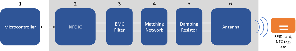
If you’re considering designing your own NFC reader, there are a few essentials you need to keep in mind. First, you’ll require an NFC chip that interfaces with an antenna for data transmission and reception. Various chips are available, with different levels of integration. You need the antenna itself, as well as the circuitry between the antenna and the NFC chip. You also need a microcontroller to process the data and communicate with other devices. And don’t forget to consider the software side, as firmware will be required to manage the interactions between the reader and the NFC tags. We'll take a quick look now at each of the components as shown in the image below.
1) We'll be starting with the microprocessor. This is the brains of your design, which handles high-level logic, manages communication with the NFC controller chip (via I2C, SPI, or UART), and processes data exchanged with the tag. It also interfaces with the user (buttons, display, etc.) or a network if your project is connected. This means you have plenty of options here, it just needs to have hardware support for the communication protocol the NFC chip uses, and be fast enough to handle the NFC stack and application logic. That's true of pretty much all of the popular hobbyist choices such as variants of ESP32, STM32 and AVR.
2) The most daunting part for most hobbyists is when it comes to the NFC chip itself. This is the chip responsible for generating the RF signal, modulating and demodulating data, and handling the low-level NFC protocol (like ISO14443 or ISO15693). It acts as the bridge between the analog RF world and the digital processor. There are a couple of popular choices out there that have been made into cheap development boards and modules, and these are the ones that is used in virtually all guides and tutorials online. The absolutely most prolific is the MFRC522 (also known as RC522 when sold as a module), followed by the PN532. These are both widely available, cheap, and have working Arduino libraries, which is important for the hobbyist market out there. For these reasons it's very likely that you've become interested in NFC after testing e.g. a RC522 module and now are here reading this post. There's important built-in features that some chips have and some don't, like collision detection and power control. And some of the older NFC chips does not support either all the modes (such as reader mode, peer-to-peer, card emulation) or support all the newer tag types. We'll use MFRC522 as an example in this post, and one of the limitations of this chip is it's limited to only detecting tags that are ISO14443 compliant (i.e it's not able to read ISO15693 tags). But the RC522 module is so cheap and so prolific that it should be within anyone's budget and availability to get their hands on one and start getting to know how to use it and it's publicly available libraries. And having a working reference design available is a big advantage when you are troubleshooting your own designs.
3) The NFC chip doesn't generate nice clean sine waves at the exact frequency we want. Instead it just pushes out a square wave at our wanted frequency. That means we get all the harmonics as well at the higher frequencies, and that is not something we want as they are not useful to us, and introduce noise into our system. The EMC filter is introduced then as a necessity to filter out all the unwanted frequencies and let us proceed with the 13.56 MHz sine wave we want. We'll dive into the circuithings on designing the EMC filter in another post. Also important, although not part of the antenna design, are decoupling capacitors close to power pins.
4) Matching network. This small network of capacitors and inductors sits between the NFC chip and the antenna. Or between the EMC filter and antenna is more accurate. It is often mistakenly lumped together with the EMC filter in blogs and tutorials. Its job is to match the impedance of the antenna to the output of the NFC chip to ensure maximum power transfer and proper resonance at 13.56 MHz, and such has a very different purpose. Matching is all about impedance transformation. While your antenna may be resonant, it won’t perform well unless it's matched properly to the chip. Matching means adapting the antenna’s complex impedance to match the input impedance of the NFC chip so that maximum power transfer occurs and maximum field strength is achieved. When mismatched, much of the RF energy is reflected back or wasted, resulting in reduced range and weaker communication. Matching is part science, part art, you estimate, you build, and you tweak, and the whole circuithings of designing and tuning the matching network for a given antenna will be the subject of a coming post.
5) Damping resistor. Designs typically have a 2-4 ohm resistor, or a 0 ohm resistor for possible future inclusions of damping, between the matching network and the antenna. The purpose of the damping resistor is widening the frequency range the antenna can couple to a tag with, at cost of H-field signal strength. Antennas can often resonate effectively very narrowly around the exact frequency it is designed for, and very poorly outside that narrow range. This can prove problematic as the presence of e.g. metallic surfaces nearby our system might detune the antenna, or the tag is detuned a bit. Meaning the antennas resonance value is shifted a bit, and our circuit then need to operate reliably at a frequency that's +/- a few % of the intended 13.56 MHz. The damping resistor widens the resonance peak from a sharp spike to a more evened out mound. So our reader works more reliably in different environments, increasing its robustness, but we trade away the maximum detection distance between reader and tag. Effectively the damping resistor means we lose more energy to heat instead of being used for communication, and lose magnetic field strength. When inserting a multiplexer or switch, it's almost always at the position of the damping resistor, and the multiplexer or switch has a certain channel resistance, such that it works just like inserting a damping resistor would have worked. Care should be taken to choose a value that balances range and robustness.
6) And lastly, the antenna. This is the heart of the reader’s RF interface. The antenna generates the electromagnetic field to power passive tags and facilitate communication. It’s usually a multi-turn loop made of copper traces or wire. The antenna directly determines how well the device couples to the electromagnetic field, how efficiently it transfers energy, and how reliable the communication will be. NFC antenna design is based on the inductive principle where the reader and tag antennas form a loosely coupled transformer operating at 13.56 MHz. Designing the antenna correctly means achieving the right inductance, tuning it to resonate at the carrier frequency, and maximizing efficiency through a good Q factor—all while keeping it small enough for your device. (The Q factor measures how sharp and efficient the antenna’s resonance is. A higher Q means better energy transfer but narrower bandwidth, which can be a problem if too extreme). For NFC systems, antennas typically have an inductance in the range of 1 µH to 2.5 µH, and that is again driven by what's practical to make size-wise. NFC readers and tags are often quite small, and since the physical wavelength of 13.56 MHz is ~22.1 meters, practically the antennas will be much smaller than the wavelength. And since the antenna is operating purely in the near field (magnetically coupled, not radiative), they don’t need to be a specific fraction of the wavelength (unlike antennas for Wi-Fi or Bluetooth).
After all of that, we're now ready to form a circuitmodel of our NFC reader design, with discrete elements for each section. The antenna section is modeled with discrete components as well since we haven't decided the antenna topology just yet.

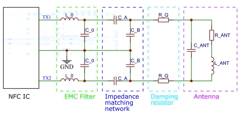
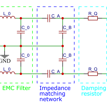
Circuitmodel of all the elements combined
Circuithings
It's all about circuit things.
contact@circuithings.com
© 2025. All rights reserved.
Contact