
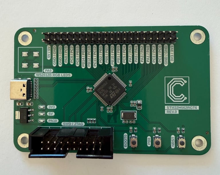
Custom STM32H562 Development Board
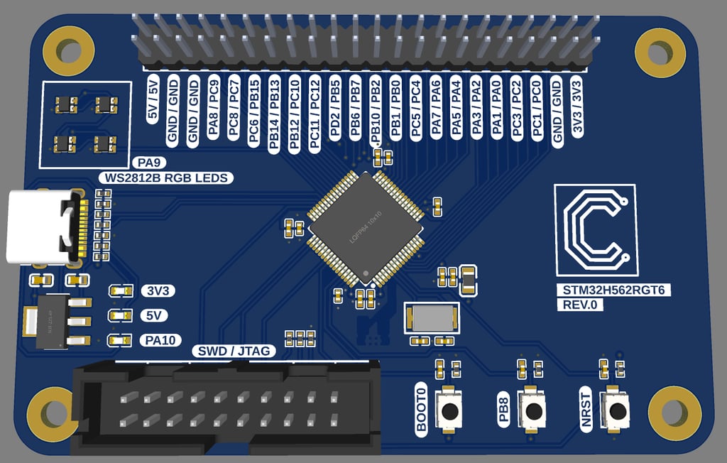
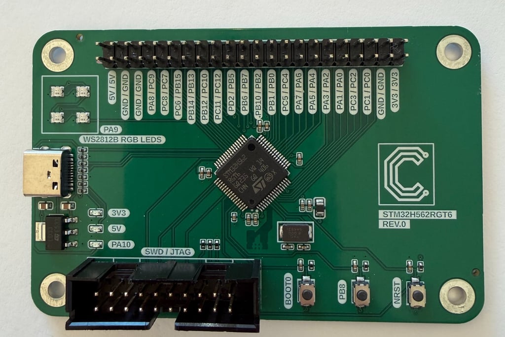
A custom development board for the STM32H562RGT6 microcontroller. The board has the complete 20-pin SWD programming interface for the ST-LINK V2 programmer, breaks out all the GPIO, has user LED, user Button, as well as a string of WS2812 RGB LEDs.
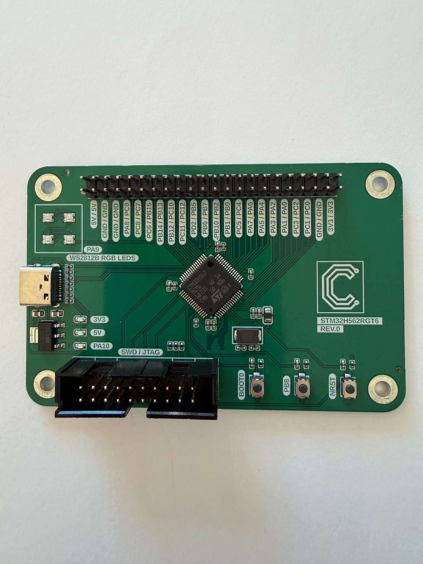
This project is primarily intended as a practical demonstration of the blog post on programming custom STM32 boards in Arduino. It uses the same basic schematic presented there, while adding a breakout header for all GPIO pins, along with a few onboard WS2812 addressable RGB LEDs. It is also intended to serve as a foundation for other projects — both for me and for anyone reading this who wants a starting point for their own designs.
The schematic from the blog post, with the addition of four mounting holes, a 44-pin male breakout header, and four WS2812B RGB LEDs:
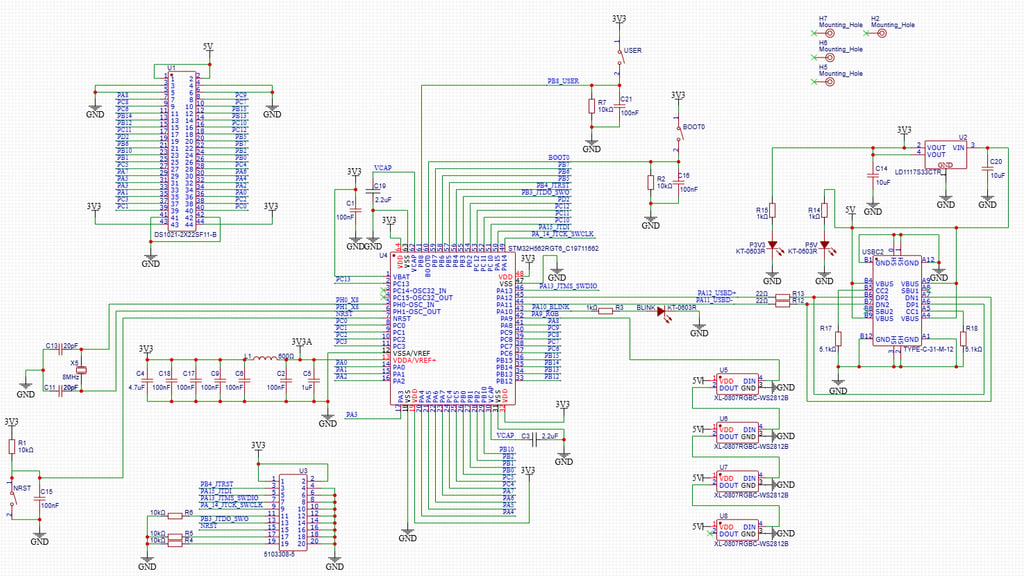
It reuses the schematic from the blog post, with component selections tailored for JLCPCB’s assembly service, using as many components as possible from the “Basic” parts library to avoid additional manufacturing costs associated with restocking the pick-and-place machines.
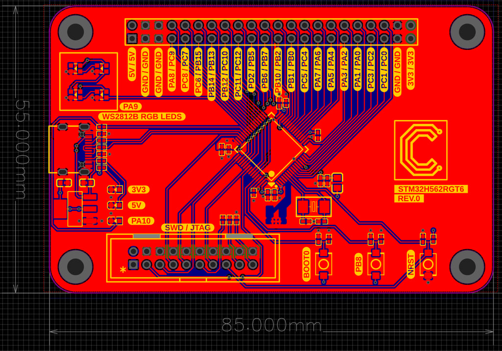
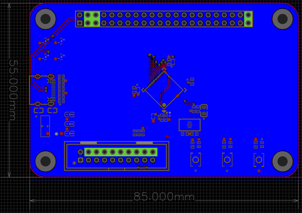
The board is approximately the size of a credit card, measuring 55 mm × 85 mm, with M3 mounting holes in each corner. As a precaution, I used a 4-layer stack-up to ensure solid grounding and power distribution for the microcontroller. More advanced STM32 chips can be somewhat more demanding in terms of PCB layout than simpler chips such as the ATmega328P, and small 4-layer boards from JLCPCB are not significantly more expensive these days than 2-layer boards.
The only drawback is that my preferred black solder mask is not included as a standard option for 4-layer boards and is instead surprisingly expensive, which is why I chose the standard green solder mask for this board.
The stack-up is mainly:
Top: Signal / GND
Inner 1: GND
Inner 2: GND
Bottom: 3V3 / Signal
There is also some additional 5V routing on the top and bottom layers. The number of traces on the bottom layer has also been kept to an absolute minimum.
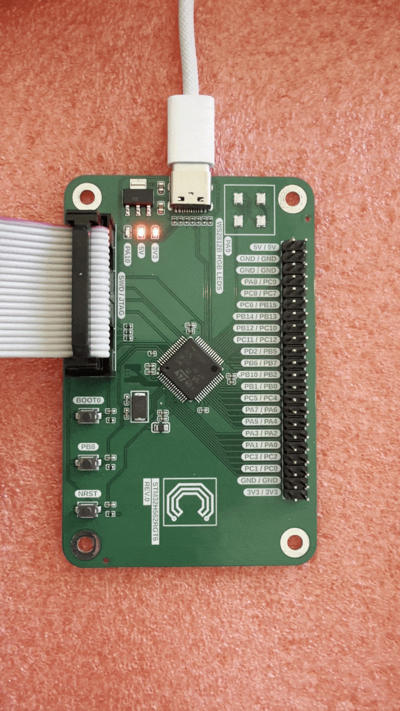
The finished manufactured board got delivered and didn't have any glaring issues. Time to test!
The first test was to supply power through the USB-C connector, connect the ST-LINK/V2 programmer, and verify that the Arduino IDE could successfully upload and run a basic sketch that blinks the user LED on PA10 when the user button on PB8 is pressed:
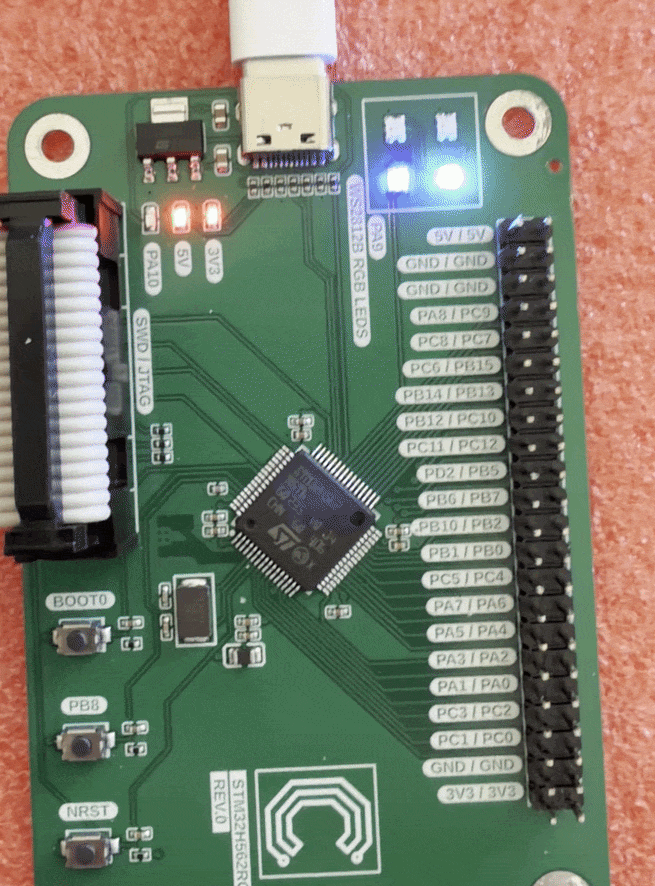
After successfully running the button-and-blink test, I tried a sketch that cycled through the four onboard WS2812B RGB LEDs using the example sketch “RGBWstrandtest” from Adafruit’s NeoPixel library. That worked exactly as intended:
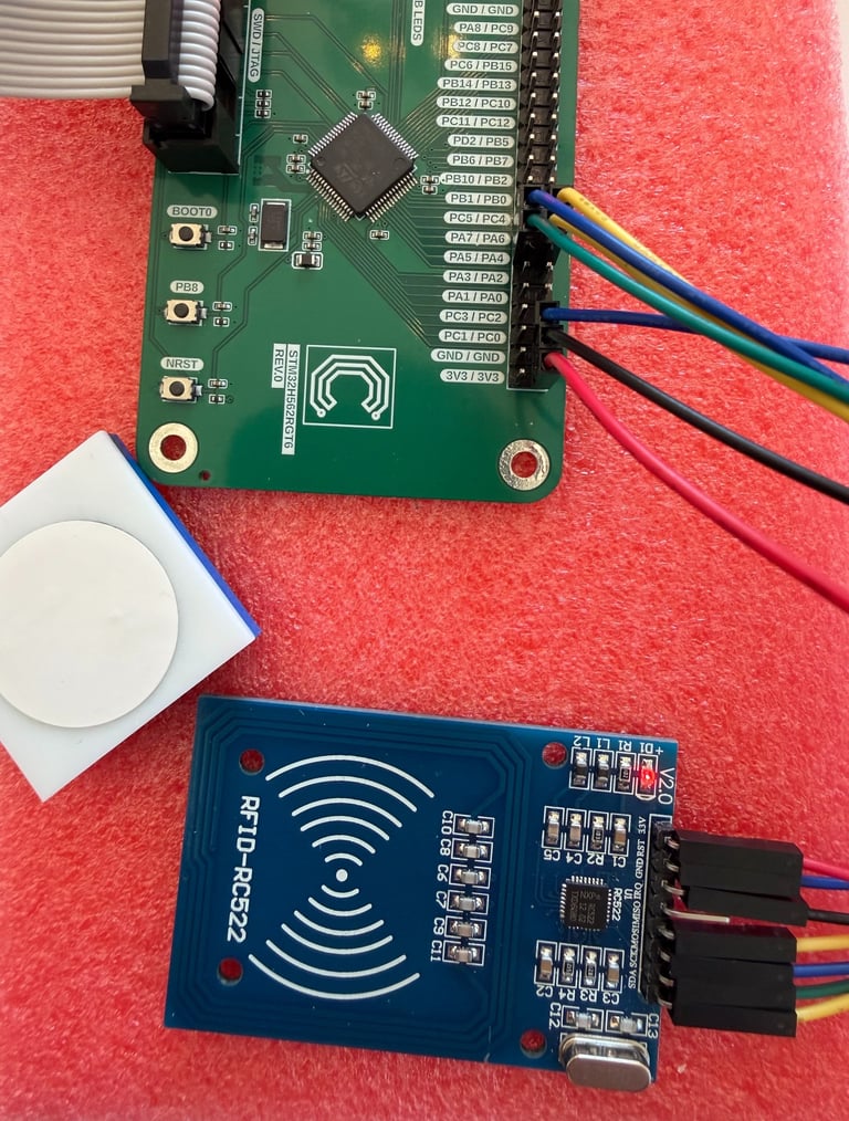
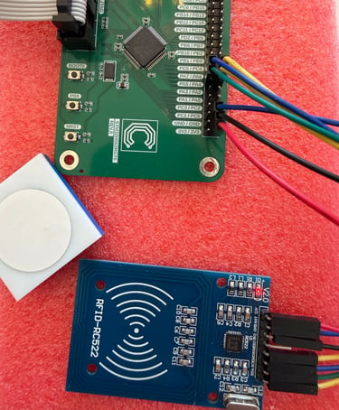
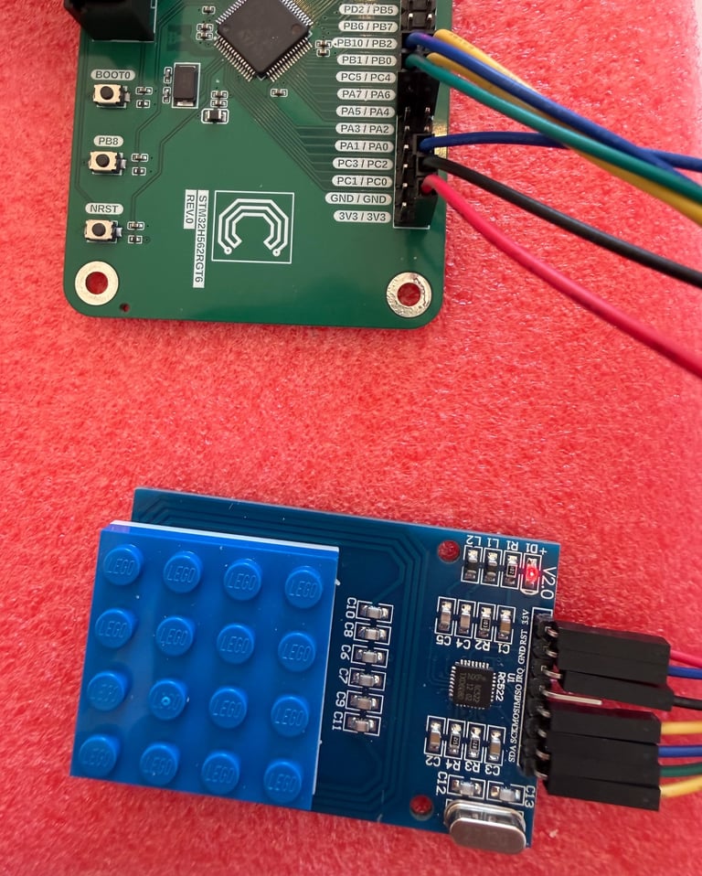
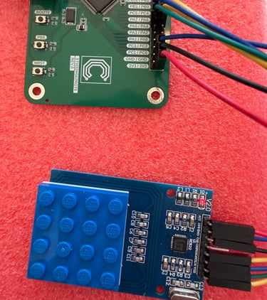
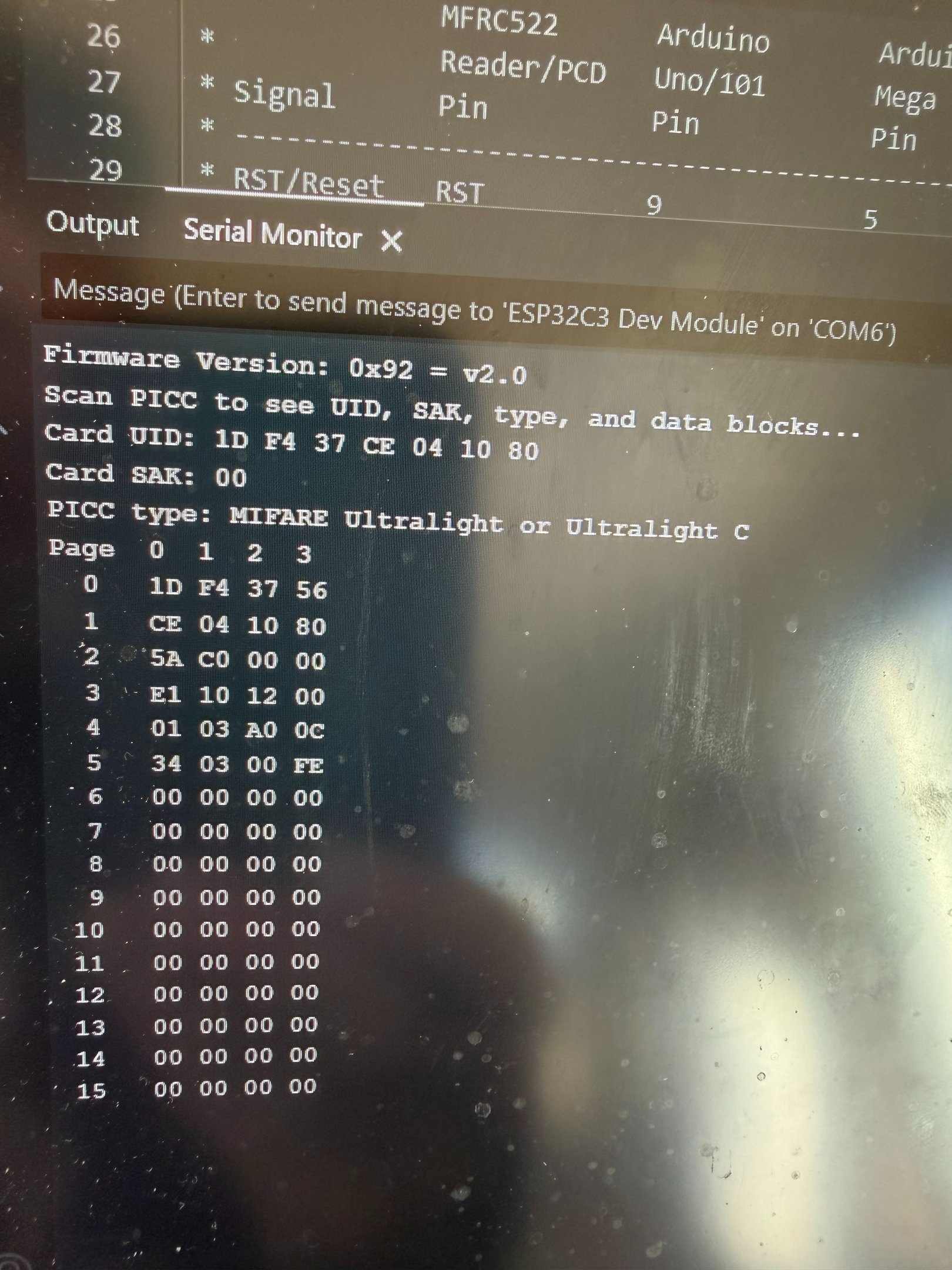
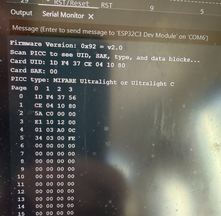
Finally, I tested an RC522 module to verify that the default SPI pins were accessible through the external pin header connection. I used the “DumpInfo” example sketch from Miguel Balboa’s RC522 library. The default pins for SPI1 are SCK–PA5, MISO–PA6, MOSI–PA7, and NSS–PA4. In addition, I needed to choose a reset pin, for which I used PC0.
In the images below, an RC522 module is connected to my board, and a basic NFC tag sticker attached to a brick is used to test reading tag information. By enabling the serial interface over CDC from the Arduino IDE Tools menu, I was able to verify that the SPI interface was functioning correctly:
Circuithings
It's all about circuit things.
contact@circuithings.com
© 2025. All rights reserved.
Contact