
Multiplexing NFC Antennas
A demo project for demonstrating how multiple NFC antennas can easily be driven and multiplexed by a MFRC522 controller and a microcontroller

The cost of a single NFC reader chip such as the MFRC522 — which I’ve used in other projects and which serves as the entry point for many hobbyists — is acceptable in small numbers, but it starts to get expensive if you want NFC sensing in multiple areas of your projects. You start wondering why you can’t just use one reader chip and switch between multiple antennas instead. At least, that’s what I thought.
And if you’re like me, you start looking around online to see how other people have done it. What you end up finding is lots of people on forums asking how to do it, followed by replies explaining how difficult it is, with plenty of RF jargon thrown in. It seems to have had a discouraging effect, as there are very few actual hobbyist projects showcasing antenna multiplexing. What we’re left with are application notes from vendors that focus on proper 50-ohm lines, matching networks, and expensive RF switches. That can also feel discouraging, since it becomes both expensive and complicated to adapt to your own projects. There are very few quick and easy solutions that are easily adaptable, and very few guides on the topic as well.
That is my motivation for making this demo project: basically showing how easy it can be if you understand what you’re trading away for ease of use.
Next, I decided to make an interface that works with an Arduino Uno, since it is still the starting point for most hobbyists. And if you’re skilled enough to use other microcontrollers, you’re probably skilled enough to make the necessary adjustments to this project to suit your needs. I also decided to keep using the MFRC522, since the Arduino library and hardware interface will likely be the most familiar options for the majority of hobbyists out there.
The next step was deciding on the actual multiplexing method. To keep the simplicity going, I’m going to use analog multiplexers with as low an on-channel resistance as I can find while still keeping them relatively affordable. By inserting the analog multiplexers right after the matching network, they either completely shut off access to an antenna or add a small resistance between the antenna and the matching network.
If you remember the blog post where damping resistors are discussed, you’ll recognize that the on-resistance introduced by the analog multiplexer behaves in a similar manner. The impedance matching network transforms the load impedance to the source impedance, and in a loss-free transformation all components should ideally be reactive elements. Adding resistance introduces a component with real power loss.
The drawback of introducing too much resistance is that a larger portion of the power sent from the NFC chip is dissipated in the resistance itself, leaving less power available to drive the antenna. As a result, the effective reading distance is greatly reduced. The resistance introduced by the analog multiplexer — again, similar to a damping resistor — forms a voltage divider with the antenna impedance. The larger the damping resistance is compared to the antenna impedance, the smaller the fraction of power delivered to the antenna.
This becomes a cost tradeoff: lower-resistance analog multiplexers are more expensive, but we don’t want to choose one so expensive that it costs as much as — or more than — simply adding another MFRC522 instead. Ideally, one analog multiplexer with, say, four channels should be cheaper than four NFC reader chips and all the additional circuitry required for them. Since typical damping resistors in NFC designs are often around 2–4 ohms, that seemed like a good place to start looking.
After browsing the JLCPCB assembly library, I found the ADG704BRMZ-REEL7 from Analog Devices, which provides a worst-case 4-ohm on-channel resistance at room temperature with a 5 V supply. At the time of writing, it costs $1.11 compared to $3.59 for the MFRC522. It also provides up to -60 dB off-isolation and a 200 MHz bandwidth, which I believe is sufficient for this application. The capacitive loading also appears acceptably low, since a few multiples of roughly 50 pF likely won’t noticeably affect the impedance matching network.
Having an Enable/Not-Enable pin also means that multiple multiplexers can be combined to multiplex even more antennas by simply adding one extra digital signal for each block of four antennas.
Since the device has a single input channel with four switchable outputs, we need two of them in parallel to handle the differential output of the MFRC522. For this demo project, that gives us three additional antennas for only about $2.20 extra. I’m actually using four multiplexers in the design instead of just two, to demonstrate how multiple multiplexers can be combined and to provide a starting point for people who may want to scale the design even further.
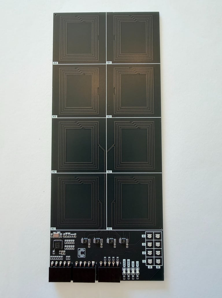
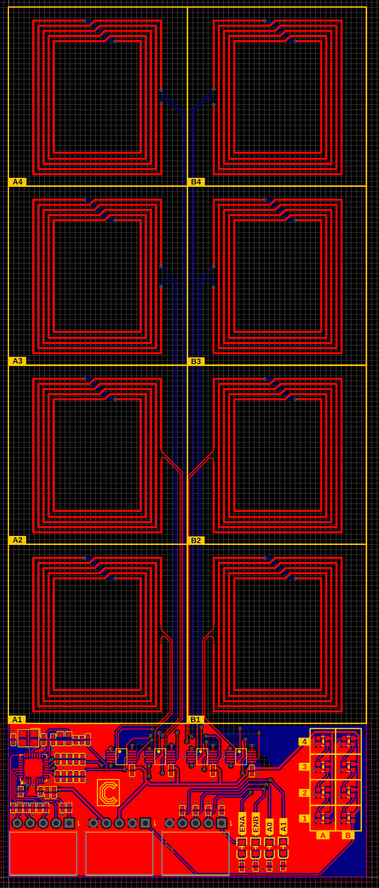
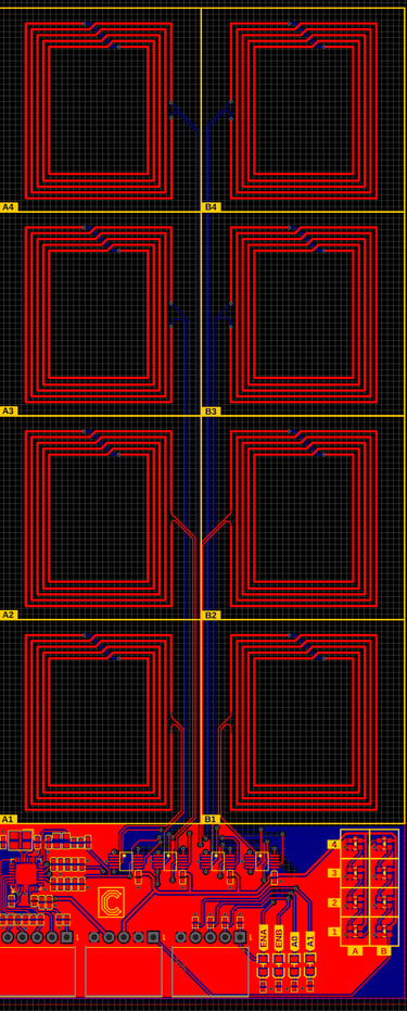
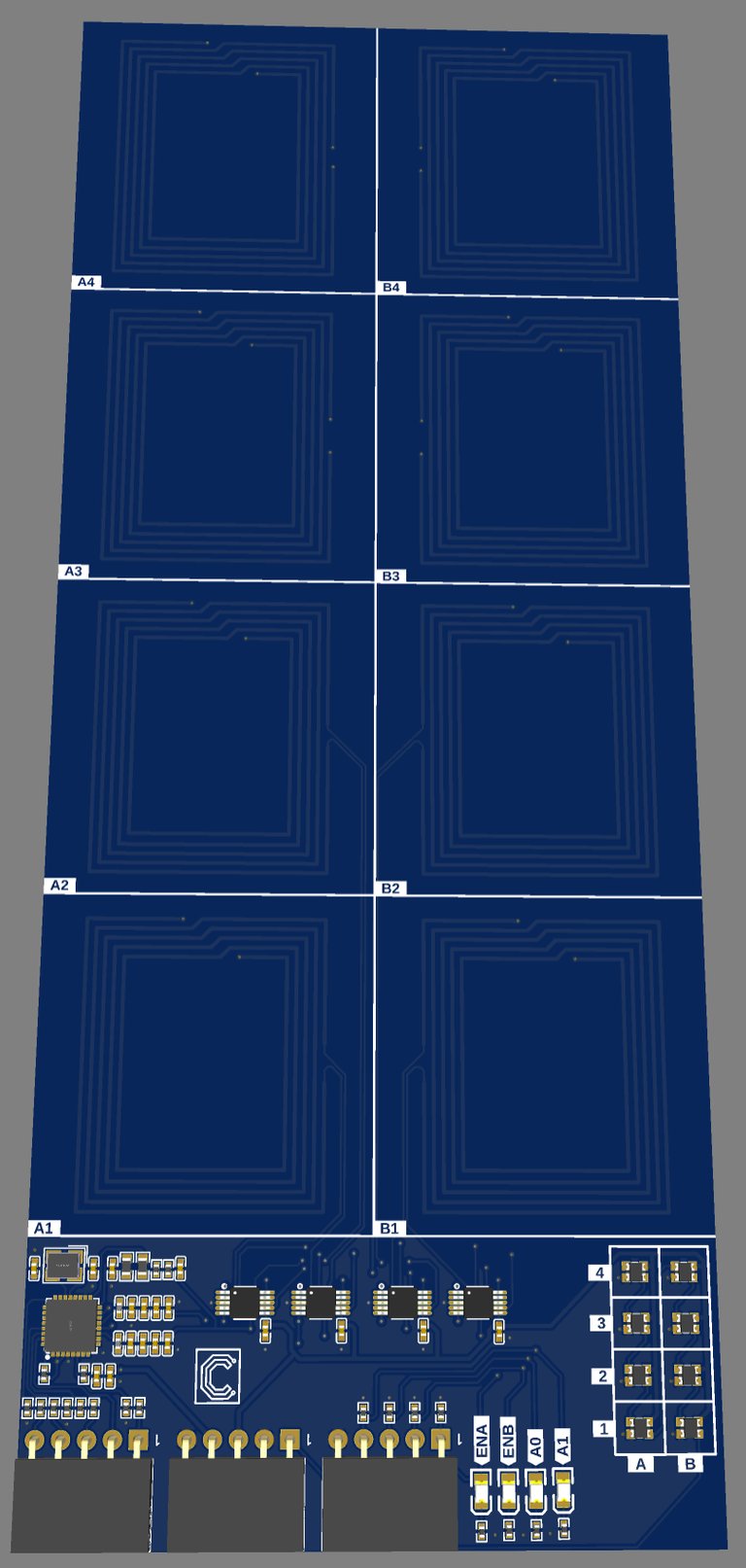
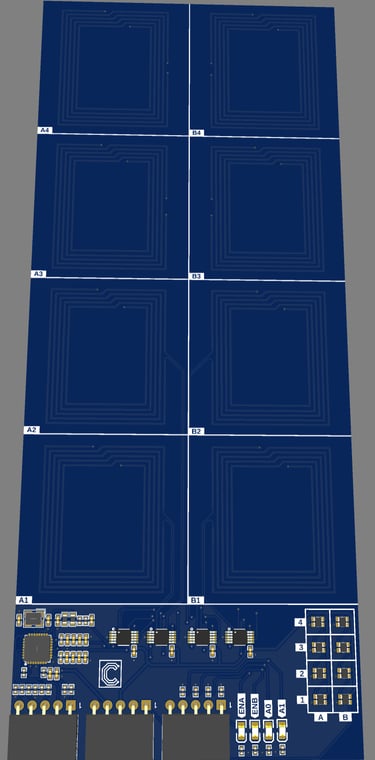
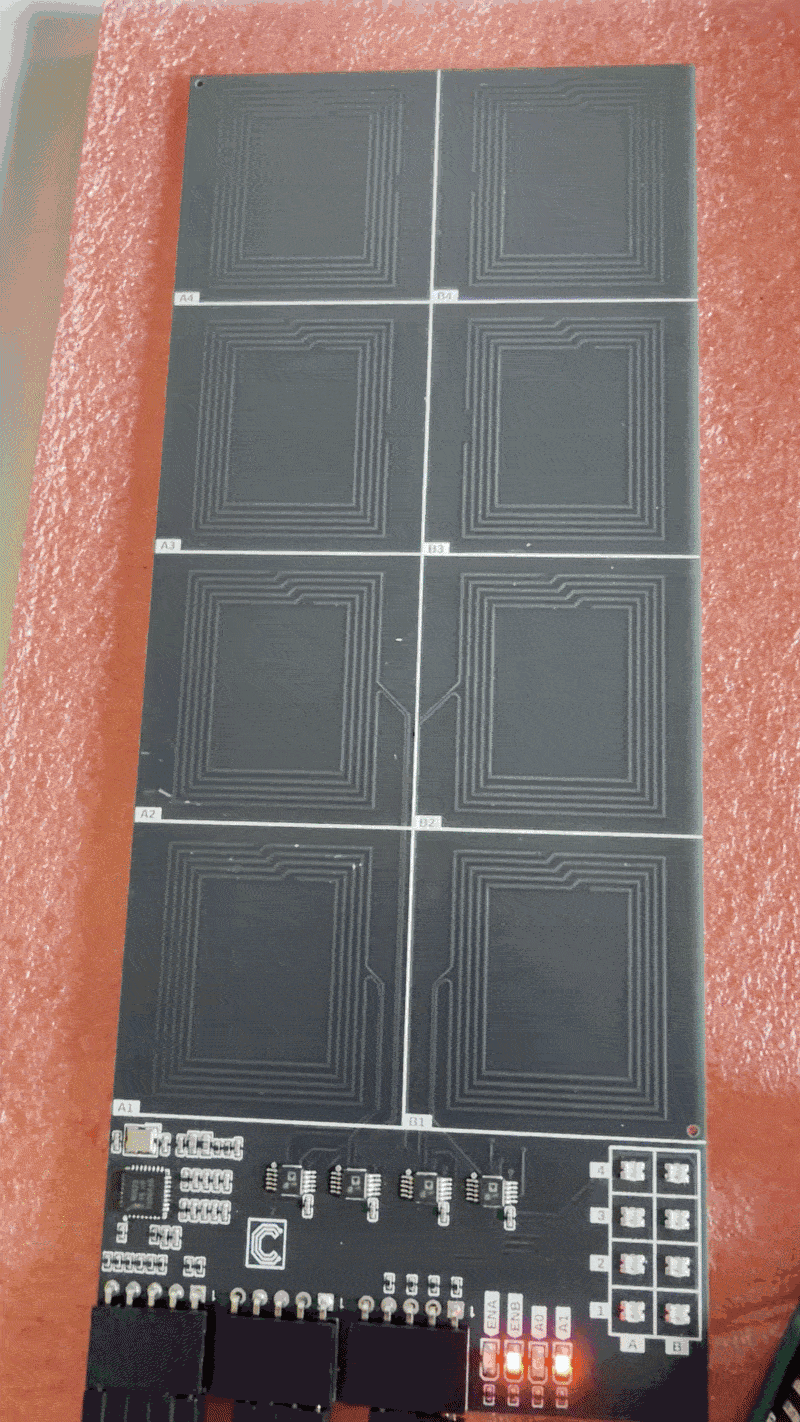
That gives us eight antennas total, arranged in a 2×4 grid. Now we’re at seven additional antennas for only about $4.40 extra — much better than adding seven more individual readers, which would cost $3.59 × 7, for a total of $25.13.
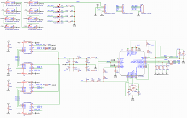
That gives us a starting point for the schematic. We need the MFRC522 and its control signals, along with the analog multiplexers and their control signals. Since we’re interfacing with an Arduino Uno, and the Uno is a 5 V device, we need to step down the SPI signals going to the NFC chip.
The options are either a proper level-shifter IC or discrete circuitry. For the sake of simplicity, I’ve just used resistor dividers here, since they work fine with the default low-speed SPI signals. If I were making another project, I’d probably choose a more robust solution that would also work well with higher SPI clock speeds, but for demonstrating the multiplexing concept it isn’t really necessary.
Finally, I added a few LEDs to show the state of the multiplexer control signals, along with some WS2812 addressable RGB LEDs arranged in the same grid as the antennas to visually demonstrate NFC tag occupancy more clearly.
The schematic then looks like this:

The PCB design uses a 2-layer stack-up where the areas not occupied by the antennas use GND pours on both the top and bottom layers, while the 5 V and 3.3 V rails are routed using thick traces on the top layer. Signal routing is done primarily on the top layer, and only sparingly on the bottom layer, in order to keep the ground plane as continuous as possible.
The areas occupied by the antennas are kept free of copper, except for a few signal traces. The antennas themselves are designed with a rectangular shape to provide enough space for routing traces between them. The main parameters used to tune the antenna impedance are the track width, the number of turns, and the spacing between the turns.
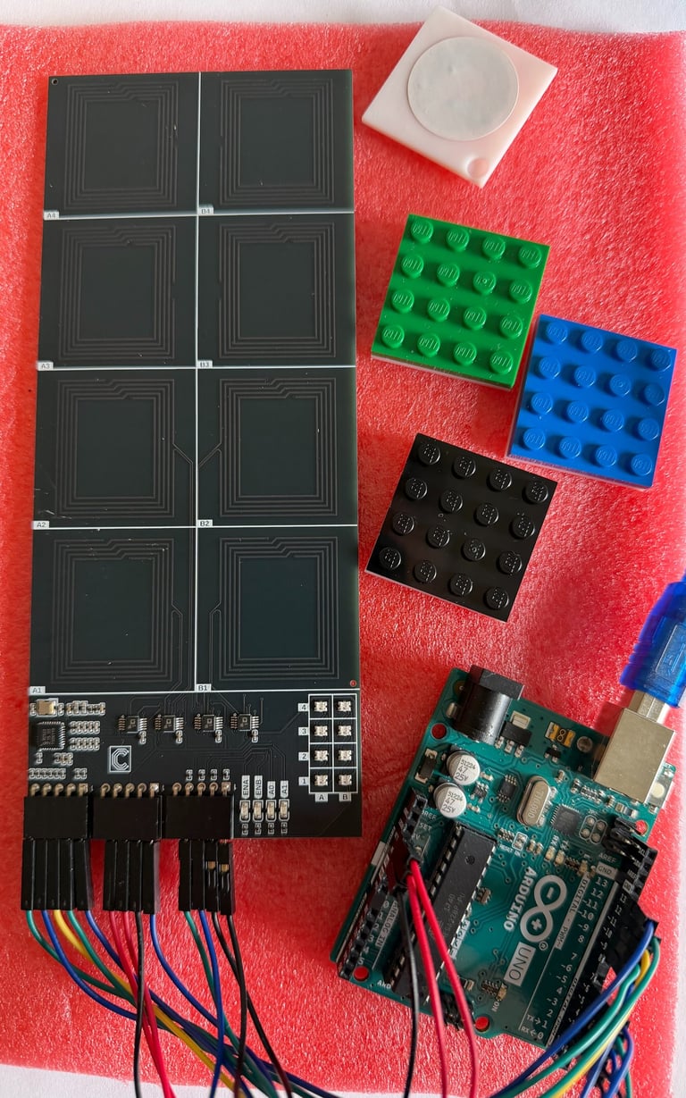
The test is basically hooking up everything and seeing that the multiplexing action work. Here's the setup, with an Arduino Uno and 4x tags differently colored LEGO plate pieces each with a tag beneath (as seen on the white one lying upside down).
I did a second test to time the execution of one full loop and the effect of having/not having a tag present.The code can be found at the bottom of this post. The results showed the following reading speeds/times:
No Tags present: 203 ms
1x Tag present: 307 ms --> 104 ms added for reading tag
2x Tags present: 412 ms --> 105 ms added for reading tag
3x Tags present: 517 ms --> 105 ms added for reading tag
4x Tags present: 621 ms --> 104 ms added for reading tag
5x Tags present: 729 ms --> 108 ms added for reading tag
6x Tags present: 833 ms --> 104 ms added for reading tag
... Ran out of tags - didn't test for 7x and 8x
Giving a accumulated switching time for swithing through all the antennas, and timing out when looking for (and not finding) a tag on each tile, of 203 ms. Thats about 25 ms. each tile. The time spent on a tile if a tag is found goes up from approx. 25 ms. to approx. 130 ms. (25 ms + 105 ms) due to communication with the Tag for reading out the basic ID information. So there's a baseline time for looping over all antennas that is approx 203 ms., and an added time of approx. 105 ms. for each tag present on the antenna matrix. The variance seen through multiple tests is between a minimum of 103 ms and maximum of 110 ms - with 104 ms and 105 ms occuring about 90% - 95% of the time.
Code for occupancy testing:
Code for timing testing:
I wrote some quick code that loops over all eight antennas and uses the onboard WS2812 RGB LED matrix to show which tile is occupied by which tag ID, and which tiles are empty.
The tags used are marked with different colors, and the tag IDs are hardcoded in the firmware together with their corresponding colors, allowing the onboard WS2812 RGB LED matrix to indicate the occupancy of individual tags.
The multiplexing and switching between the tiles is controlled by toggling the ENABLE pins and the address lines A0 and A1 high and low, which is indicated by the LEDs rapidly flickering at the bottom of the PCB.
The code can be found at the bottom of this post.
Circuithings
It's all about circuit things.
contact@circuithings.com
© 2025. All rights reserved.
Contact